
For the last two years, the conversation about AI infrastructure has lived inside a narrow frame. Investors debate GPU shipments. They track advanced packaging capacity. They argue about hyperscaler capex and cloud backlogs. The frame has been useful, but it stops one layer short of the actual constraint.
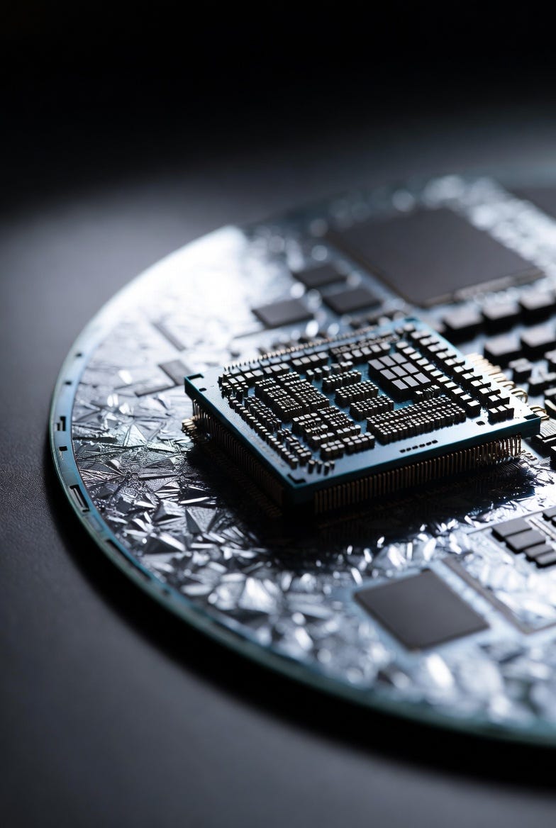
Beneath every advanced chip sits a polished disc of silicon, roughly the size of a dinner plate. For leading edge logic, that disc is not the working surface. It is the structural substrate. The working surface is a much thinner layer grown on top of the disc, only a few microns thick, called the epitaxial layer.
Picture an ice rink. Beneath the ice sits a concrete slab that nobody ever skates on. The slab provides the structure. But the skating happens on the inch of perfectly maintained ice laid down on top, every part of it the same thickness, every part of it free of cracks. A single defect in the ice and the rink cannot host a competition. The slab without the ice is a parking lot. The ice without the slab has nothing to rest on. The two work together, but the function lives in the layer on top.
The wafer is the same idea. The polished disc is the slab. The epitaxial layer is the ice. Every transistor in an advanced chip is grown into that thin layer, not into the disc below it. The disc holds it up. The layer is where the work happens.
This is why the epitaxial step matters so much in the conversation. The defect tolerance required at three nanometres and below cannot be achieved on a polished disc alone. The crystalline structure of the epi layer has to be near perfect, grown atom by atom in a dedicated reactor, qualified to specifications that can take eighteen months to certify on a new production line. It is not a coating. It is a precision crystalline overlay, and it is the actual real estate that every advanced foundry pays for. The wafer is not a commodity. It is a precision input made by a small handful of companies in the world, sold under multi year contracts.
Right now, the leading edge variant of that wafer is sold out. Existing 300mm capacity at the relevant suppliers is running above ninety five percent utilization. Customer inventory at the high end is reported to be near zero. The long term agreements signed in 2023 cover well over half of available supply through the end of 2027. And demand for these wafers is growing above twenty percent per year, materially faster than any plausible supply response.
This is the layer the market is not watching. This is where the next repricing event in semiconductors is going to occur. And it is going to occur on a contractual schedule that is already public information, sitting in plain sight in supplier filings, customer transcripts, and industry data nobody has bothered to put together.
I find this kind of setup rare.
What sits beneath the chip
When investors think about the AI supply chain, the picture usually ends at the foundry. The leading edge logic process. The advanced packaging step. The high bandwidth memory stack. These are real bottlenecks. They have been written about extensively. They occupy the financial press and the analyst notes for good reason.
But the foundry does not start with a finished input. It starts with a wafer. And the wafer industry is structured very differently from the layers above it.
There are essentially a handful of companies in the world that produce 300mm silicon wafers at scale. Together they constitute a tight oligopoly. They have done so for decades. The barrier to entry is not capital. The barrier is qualification. A new wafer line takes two to three years to deliver its first wafer and another twelve to eighteen months to be qualified by the customer. Each customer has its own inspection standards, its own defect tolerances, its own audit process. Once qualified, switching is painful for both sides. The relationship is sticky in a way that does not exist in most parts of the technology supply chain.
This produces the pricing structure that defines the industry. Customers sign long term agreements, typically five years in length, that lock in volume and base pricing. The agreements include modest annual escalators, usually two to three percent. Spot pricing exists at the margin for premium products, but the bulk of supply moves at contracted rates. The 2023 round of agreements set the prices at which the world is consuming its current wafer supply. Those agreements expire at the end of 2027.
This matters because the conditions under which the 2023 agreements were signed are not the conditions under which the next round will be negotiated. When the 2023 contracts were drafted, AI demand for leading edge silicon was a rounding error. Foundry utilization at the leading edge was healthy but not extraordinary. Memory was in a downcycle. The wafer suppliers were focused on managing inventory, not on rationing capacity.
Today, every one of those conditions has reversed. The suppliers walk into the 2027 negotiations from a position of structural strength they have not enjoyed in a decade.
The demand inflection
The numbers on the demand side are striking once you separate them from the noise.
Industry models suggest that AI related leading edge wafer demand has gone from roughly 250,000 wafers per month in 2023 to approximately 600,000 wafers per month in 2026, and is projected to approach one million wafers per month by 2028. That is a tripling in three years and a quadrupling in five. It is one of the steepest demand curves in the history of the industry, and it sits on top of a supply base that has been deliberately starved of capital since the 2022 to 2024 downcycle.
The reason the curve is so steep is not just unit growth. It is silicon intensity. An AI server consumes roughly four times more silicon than a conventional server in surface area terms. Each of the most advanced chips is increasingly being manufactured using two wafers rather than one, owing to architectural shifts like backside power delivery and three dimensional packaging. This is not a marginal change. It is content growth on top of unit growth, multiplying through the same supply chain.
High bandwidth memory adds a second, independent vector. HBM uses standard polished wafers rather than the epitaxial variant required for logic, but the unit growth is just as severe. Industry data suggests HBM alone now represents slightly more than five percent of the global 300mm wafer market, a share that has effectively appeared from nowhere over the past three years. The trajectory is accelerating. Memory has gone from being a footnote in the wafer demand picture to a meaningful tailwind in its own right.
Combine the leading edge logic story with the high bandwidth memory story, and AI driven demand for silicon wafers is now well above ten percent of the total 300mm equivalent market. By the end of the decade that share is expected to roughly double.
There is one number that anchors the magnitude of this shift. AI specific chips represent less than half of one percent of global wafer starts but already generate about a fifth of total semiconductor revenue. The disproportion between volume and value has never been wider in the industry. It tells you, in clean arithmetic, where the marginal dollar is being earned and where the binding constraint is going to bite.
The supply cap
The supply side cannot respond on the timescale that demand is moving.
Building a new wafer line is not the same as building more chip capacity. A greenfield wafer fab capable of adding roughly one percent to global supply costs between one and two billion dollars. That is small relative to the cost of a leading edge logic fab, which can run twenty to thirty billion. But the cost is not the binding constraint. The binding constraints are time, qualification, and equipment lead times.
A new line takes two to three years to produce its first qualified wafer. Customer qualification adds another twelve to eighteen months. The dedicated equipment required for the epitaxial step, particularly the reactors that grow the crystalline layer, has lead times measured in many months from the equipment supplier. Cleanroom space is itself constrained. Even the firms that want to expand cannot do so on a calendar that matters for the 2027 cycle. Any decision to add incremental capacity made in mid 2026 does not produce a sellable wafer before the second half of 2027 at the earliest. The decision to add capacity for the 2028 negotiations was already late by the time it was being considered.
The capital intensity of the previous cycle did not help. Industry capex peaked in 2023 at the top of the previous greenfield wave and has since fallen approximately seventy percent. Management teams across the wafer industry have guided to lower capex in 2026 and have signaled that the trend continues into 2027. The depreciation burden from the prior wave is suppressing reported earnings, which has dampened market enthusiasm and further restrained any appetite for new builds. The supply discipline is real, and it is largely involuntary. The companies in this industry have been punished by the equity market for the last cycle’s over building, and they have responded the way disciplined operators always respond. They have stopped building.
The result is an oligopoly with finite capacity, no incentive to break ranks on pricing, and a binding constraint that cannot be wished away with capital alone. China, which now represents over twenty percent of global 300mm equivalent capacity, is not relevant to this conversation. Domestic Chinese capacity is qualified for mature nodes only. The first competitive Chinese leading edge product is not expected before 2027, and even that timeline is generous. The customers who require leading edge wafers in 2027 will be buying from the same handful of suppliers they buy from today.
The 2027 reset
This is the part of the picture that the consensus has not absorbed.
The current long term agreements expire at the end of 2027. Renegotiations will occur in early 2027. The customers walking into those negotiations are the most capital intensive companies in the world, and they have been telling the market for two years that their AI roadmaps depend on access to these wafers. The suppliers walking into those negotiations are sitting on capacity utilization above ninety five percent, customer inventory at near zero, and a backlog of demand they cannot fill at any price. The leverage in the room has reversed.
The previous cycle that most resembles this one is the 2017 wafer ASP move. The setup then was nearly identical. A multi year period of weak demand and capex restraint had left the supply base structurally underinvested. A series of demand shocks then hit at once. The first hyperscaler buildout. The transition to 3D NAND. Smartphone content growth. SSD adoption. The supply base could not respond. Industry ASPs moved approximately twenty percent in the next round of contract negotiations. The wafer makers saw the largest pricing reset in over a decade, and the equity returns in the names exposed to leading edge ran several multiples of the broader semiconductor index between trough and peak.
The 2027 setup carries the same template with a heavier demand vector. AI infrastructure spending is larger, more concentrated, and more contractually committed than the hyperscaler buildout that drove the 2017 move. The silicon intensity per server is materially higher. The HBM tailwind is a second independent driver that did not exist last time. The supply response has been weaker, not stronger, than it was in the prior cycle. The conclusion is straightforward. The 2028 wafer ASP move should be in the same range as the 2017 move at the conservative end and meaningfully larger if any of the demand vectors surprise to the upside.
The Street is not modeling this. Consensus appears to be anchored to a framework of broad market oversupply in 2025, leading edge tightness in the second half of 2026, and a general recovery toward the end of 2027. Most analyst models assume mid single digit ASP growth in 2028. That is roughly a quarter of what the 2017 analog implies. The gap between the consensus number and the structural setup is the entire investment opportunity.
The reason for the disconnect is timing. Reported earnings at the wafer suppliers are likely to look weak through the end of 2027. Depreciation from the 2022 to 2024 greenfield wave hits the income statement in the very period when ASPs are still constrained by existing contracts. Investors looking at trailing earnings will see a depressed number. Investors looking at the 2028 setup will see a step function. Markets reward what they can already see and discount what requires looking eighteen months out. That is precisely why the opportunity exists at all.
Why this matters more than the chip story
The chip layer of the AI infrastructure conversation has been widely covered. The packaging bottleneck has been widely covered. The grid bottleneck has been widely covered. Each of these is real, and each has been priced, at least partially, into the equity prices of the obvious beneficiaries.
The wafer layer is different. It is structurally further upstream. It is concentrated in a smaller number of suppliers. It moves on a contractual timetable that is largely public, available in supplier filings and industry research, and yet largely unreflected in current valuations. The wafer suppliers do not headline conference keynotes. They sell a precision input that the world treats as a commodity, even though every page of the technical documentation insists it is not.
This is the kind of mispricing I look for. It is not a story of speculative hope. It is arithmetic on a calendar. The contracts exist. The renewal dates exist. The capacity utilization is reported. The demand vectors are documented. The supply response is constrained by physics and by lead times that cannot be compressed. Every variable is observable. The only step the market has not taken is to put the variables together.
The framework is what I trust. None of this is a guarantee. Cycles can shift. Demand can soften. Specific suppliers may execute well or poorly through the period. But the structural conditions, in my reading, favor the asset class as a whole more cleanly than they have at any point since the prior reset.
Risks
Three risks deserve serious consideration before any of this becomes actionable.
The first is China. Chinese 300mm equivalent capacity has grown roughly five times since 2021 and now sits at over two million wafers per month. Almost all of it serves domestic mature node fabs. None of it is qualified for leading edge production. But it places a structural ceiling on lagging edge wafer pricing and prolongs the inventory normalization cycle for the broader 300mm market. Investors looking at blended ASPs across all wafer types will see the lagging edge drag on the headline number. The leading edge price move will be partially obscured in the reported figures until the mix shifts enough for the leading edge to dominate the average. Patience is required. The number that reports in the first half of 2028 may not yet show the full move.
The second is inventory. Customer inventories across the broader semiconductor supply chain remain elevated. Wafer supplier days of inventory is reported in some cases above two hundred days. The leading edge tightness is real, but the broader market is still working through the inventory of the prior cycle. The thesis I have described is for the leading edge variant specifically. The broader 300mm market normalizes more slowly, and the equity prices may move with the broader picture before they move with the leading edge picture.
The third is depreciation. The greenfield investments of 2022 to 2024 are hitting the income statements of the wafer suppliers now and will continue to do so through 2027. EBIT will be suppressed across the group, in some cases significantly. Investors who screen on trailing earnings will pass over these companies. This is, in my view, a feature of the setup rather than a defect. Markets reward what they can already see. The depreciation drag is exactly the reason the equities are not trading at the multiple the 2028 setup justifies. But it does mean the holding period requires conviction. The earnings need to look bad before they look good, and that is uncomfortable while it is happening.
Closing
The pattern I have learned to trust is the one where every variable is observable and the market simply has not connected them.
In this case, the variables are not hidden. The contracts are documented in supplier filings. The demand growth is reported by the foundries themselves. The supply additions are quantified in the public capex of the wafer makers. The lead times are stated by the equipment suppliers. The 2017 analog is in the history books. The renewal dates are on the calendar.
What is absent is the synthesis. The equity market is pricing each variable in isolation. The synthesis is what produces the conviction.
I have written before that the AI infrastructure thesis is not a story. It is arithmetic. The chip layer has been priced. The packaging layer has been priced. The grid layer is being priced. The wafer layer has not.
The disc beneath the chip is the constraint nobody is watching. The supply is finite. The contracts reset in 2027. The demand has already arrived.
That is enough.
· · ·
Neel Khokhani
Founder and CEO, Epochal Corporation
@neel_epochal